If you would like an offline version of these instructions, you can download it here:
nw2s::io Unbalanced Build Instructions
OVERVIEW
This is a relatively simple build and while it should not be a first attempt at DIY, it can be tackled by anyone with some soldering experience and attention to detail. It can be completed in a matter of a couple of hours, but it’s not without it’s quirks, so please pay attention, read through the instructions and take note at some of the areas of attention that I have called out.
As I’ve said before, there are plenty of good tutorials on soldering, so I won’t go into that here. Take some time and read through Adafruit’s instead.
Tools and Supplies
Required:
- Nice soldering setup and the skills to use it!
- Lead-free solder – make the switch – for the kids!
- Lead bender
- Diagonal cutters
- 3/16″ socket driver
- 5/16″ socket driver
- paper towel or masking tape to cover driver
Recommended:
- Panavise PCB holder
Kit Contents
Take a little time to look through the kit contents and make sure you have everything. If anything is missing, just send an email.
Discretes
| Description | Count |
|---|---|
| green LED | 16 |
| sunt Regulator TL431 | 1 |
| diode 1N148 | 16 |
Passives
| Description | Count |
|---|---|
| 2kΩ resistor (red black black brown brown) | 16 |
| 33kΩ resistor (orange orange black red brown) | 16 |
| 300Ω resistor (orange black black black brown) | 1 |
| 1kΩ resistor (brown black black brown brown) | 1 |
| 3.3kΩ resistor (orange orange black brown brown) | 1 |
| 10µF electrolytic capacitor | 3 |
| 0.1µF ceramic capacitor | 2 |
ICs
| Description | Count |
|---|---|
| bipolar op amp TL064 | 4 |
| 14 pin DIP socket | 4 |
Electromechanical
| Description | Count |
|---|---|
| jacks | 16 |
| jack hex nuts | 16 |
-
Connectors
| Description | Count |
|---|---|
| 2×6 receptacle | 2 |
| 1×8 receptacle | 1 |
| 2×8 receptacle | 1 |
| 2×8 headers | 1 |
| 2×6 headers | 6 |
| 1×8 headers | 1 |
| Power header | 1 |
Other
| Description | Count |
|---|---|
| nw2s::io panel | 1 |
| Panel pcb | 1 |
| Main pcb | 1 |
| DB-25 connector assembly | 2 |
| DB-25 panel nuts | 2 |
| Eurorack power cable | 1 |
ASSEMBLY
Panel PCB
Start with the panel PCB. It’s the easiest and the best place to start for some instant gratification. The first step is to take the pin header receptacles and solder them to the bottom of the panel PCB. Note that one of the header silkscreen placements indicate that it should go on top. This is an error, so please be sure to put all of the pin receptacles on the BOTTOM of the PCB.
Start with the two dual-row headers. One is a 2×8 and the other is a pair of 2x6s. These will be the easiest to place and solder.
Once those are in place, you can do the same with the 1×8 receptacle.
Next, we’ll do the jacks. It’s easiest to do four corners and then use those to anchor the other 12. Start by placing the corners and solder them into place. Be careful with your soldering iron. The receptacles poking out the solder side like to get in the way and melt in the worst way possible. Trust me though, this is easier than the alternative!
After they are firmly affixed, you can place the rest of the jacks and use the panel to hold them in. You only need to loosely tighten the hex nuts on the four corners.

Solder them and then remove the panel.
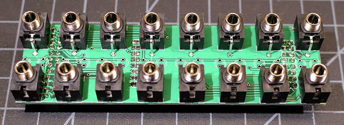
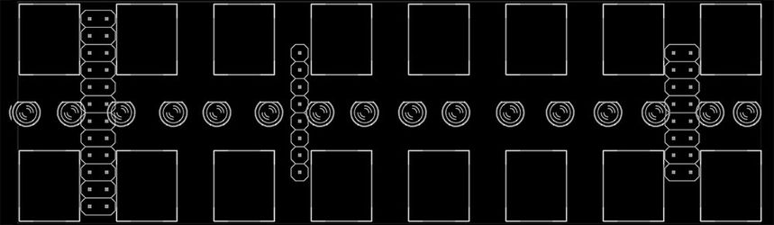
Next, you’ll want to place the LEDs. Note that the LED library I use does not do a very good job of indicating the orientation of the LED. This is unfortunate as it’s VERY important that these go in the right direction. Since the PCB doesn’t indicate, I’ve included a shot of the layer that is missing below. Note that when the board is oriented as the image shows, the flat side (negative, cathode) faces up and the long pin (positive, anode) faces down.
once they are all placed, but before you solder anything, replace the panel, flip the whole thing over, and make sure that the LEDs are all in their holes and are pushed through as far as they will go so that they are evenly poking out the other side. Make double sure and then start soldering. I will typically only do one leg of each LED in a pass so that if one gets maladjusted, you only have to reheat one leg at a time to get it to reposition.
Again, be careful of the pin header receptacles as you’re soldering. You are done with the panel, but don’t yet remove the protective film and put all the hex nuts on. You may need to debug, and if so, you don’t want to have to take them all off over and over again.
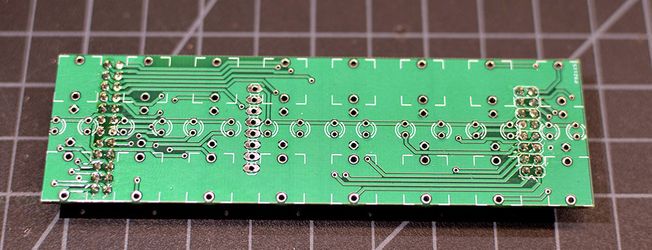
Main PCB
Set the panel to the side for now. We’ll need it to help line up some pin headers shortly.
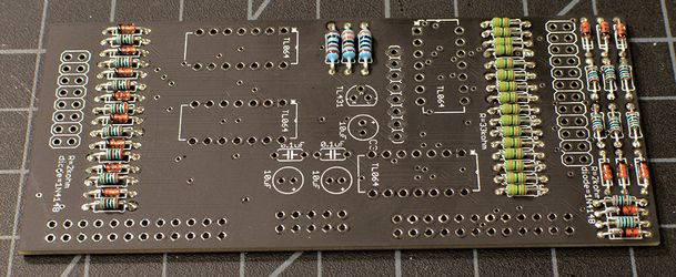
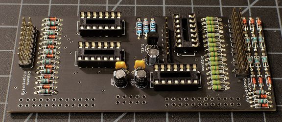
To the left you will see that the 2kΩ resistors are interleaved with the 1N4148 diodes. These are the LED current limiting resistors and reverse voltage protection.
At the very right are the second set of reverse voltage protection diodes for the LEDs.
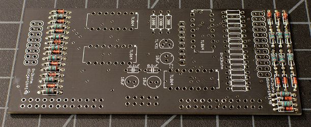
The middle three resistors set the bias voltage for the LEDs so that they will produce at least some light even with the smallest signal.
To the right of center are the resistor pads. These 33kΩ resistors are paired to provide 6dB of gain reduction. If you wish to customize the gain reduction, you may adjust the values of these resistors within reason. You will want to keep the total resistance value to a point where you will minimize the interaction with the device you will be recording with. There is no hard and fast rule. Feel free to ask.
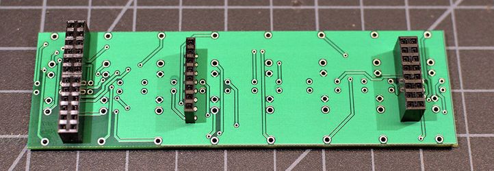
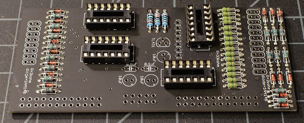
Next, solder in place the four IC sockets. Note the orientation on the board and be sure to line up the notch in the top on the same side as the asterisk that marks pin 1.
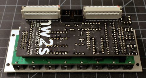
Before placing the board-to-board pin headers, you will want to insert them into the receptacles that have been soldered onto the panel PCB. Then arrange the main PCB so that they all fit together. Note that the component-side of the main board will face the solder-side of the panel board. These pin headers will be on the same side of the main board as all of the other components.
Once fit and soldered you will need to separate them again so that we can solder the final components.
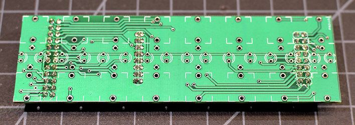
Return to the top to solder the higher components including the three 10µF electrolytics, the two 0.1µF ceramics, and the TL431 shunt regulator.
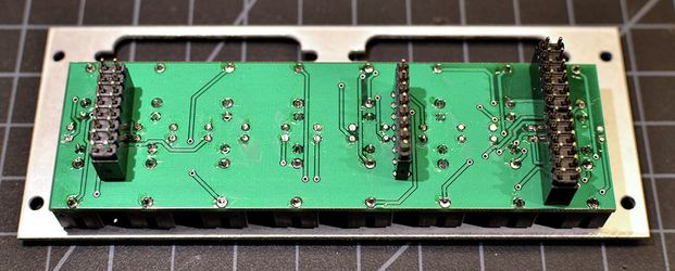
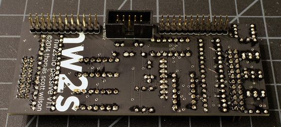
Flip the main board over and place the DB-25 pin headers and solder them so that they face downward. They will face the same direction as the power header.
Then connect the power header so that the notch lines up with the small rectangle silkscreened onto the bottom of the PCB.
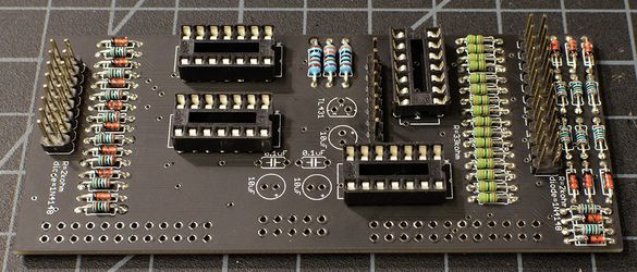
Flip it back over and socket the ICs as shown such that the notches on the op amps face the notches in the sockets. Next, we will put it all together and test it.
Assembly and Testing
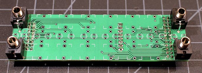
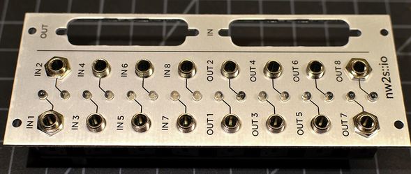
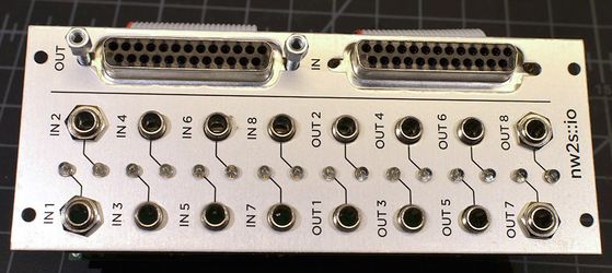
Reassemble the PCBs as shown.
Attach the DB-25 harnesses as shown, with the red stripe towards the top (right). Note that the DB-25s use a 25 pin cable and the wire-to-board connectors use a 24-pin cable. The red wire will be trimmed immediately before the board connector. This is intentional.
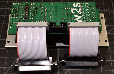
Flip it over and use the included 3/16″ nuts to attach the DB-25s to the panel. Note that we are currently still testing, so don’t remove the protective film yet, and don’t tighten it down too hard.
Once those are in place, power up the unit and to make sure no magic smoke escapes. When both the inputs and outputs are left unconnected, the op amps tend to float and may indicate a signal. Don’t worry, as soon as you have a snake connected, this will not happen.
To test signal path, you will want to start by testing the outputs. Connect a snake to the OUT port and connect all 8 outputs to your recording device. Arm 8 inputs so that you can monitor them all at once. Then, one by one, plug an oscillator into each IN jack and ensure that the signal is present on that one channel and no others.
Assuming all of the outputs pass audio, then the easiest way to test the inputs is to create a loopback where the input jacks are each connected to the output jacks. Then, using your DAW with the same setup, send a signal to each of the inputs, routed to the outputs, you should get the signal back into your DAW. Note that the signal will be about 18dB lower due to the gain reduction in the circuit, but the signal should still be audible.
Troubleshooting
So far, the only issues I’ve had with signals is that the crimps of the DB-25s can be a bit finicky. By the time you get them, however, they should be individually tested. You can double check this with a continuity tester to ensure that for each pin of the DB-25 side that neither of the neighboring pins are shorted to it.
Finishing Up
Once everything is confirmed working, you can now completely remove the panel and peel off the protective film. Replace the panel, paying attention to the LEDs, and screw on the hex nuts to all 16 jacks. When tightening, be very careful to avoid scratching the panel. I use a small square of a single layer of paper towel laid over the jack. I have seen others use masking tape attached to the nut driver. Use whichever you feel more comfortable with.
HOWEVER!!! Be aware that the nuts on the PJ301Ms to not need to be torqued down. Once the nut makes contact with the panel, turn no more than 1/4 turn further. You will feel a bit of resistance, but not a lot. Be careful.
You’re done and can now enjoy the satisfaction of 8 channels of audio or CV in and out of your typical studio or live workflow.